

As electronic devices continue to become smaller, more powerful, and increasingly complex, ensuring the reliability of printed circuit board (PCB) assemblies has become one of the biggest challenges in modern electronics manufacturing. Traditional inspection methods such as visual inspection, SPI (Solder Paste Inspection), and AOI (Automated Optical Inspection) provide excellent quality control for many production stages, but they have limitations when it comes to inspecting hidden areas of electronic assemblies.
Many modern electronic components, including BGA (Ball Grid Array), QFN (Quad Flat No-leads), and other advanced semiconductor packages, contain solder connections that are located underneath the component body and cannot be inspected using optical systems. This is where Automated X-Ray Inspection (AXI) technology becomes essential.
X-Ray inspection allows manufacturers to see inside PCB assemblies and analyze hidden solder joints, internal structures, and potential defects that would otherwise remain undetected. By providing detailed information about the quality of solder connections, AXI systems help improve product reliability, reduce failures, and ensure that electronic devices meet strict quality standards.
What is Automated X-Ray Inspection (AXI)?
Automated X-Ray Inspection (AXI) is an advanced quality control technology used in PCB manufacturing to inspect electronic assemblies using X-Ray imaging. Unlike optical inspection systems that analyze only visible surfaces, AXI technology penetrates through components and materials, allowing manufacturers to examine internal structures and hidden connections.
The main purpose of AXI is to identify defects that cannot be detected through traditional inspection methods. This includes problems inside solder joints, under semiconductor packages, and within multilayer PCB structures.
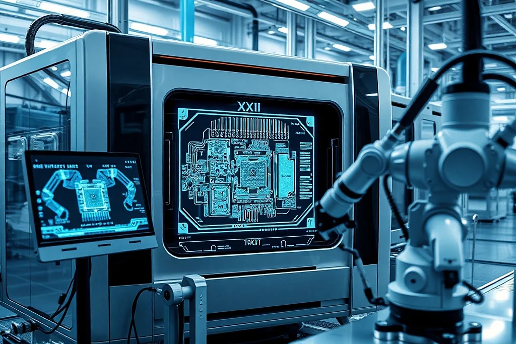
During the inspection process, an X-Ray source generates radiation that passes through the PCB assembly. A detector captures the transmitted signals and creates detailed images of the internal structure of the board. Advanced software then analyzes these images and compares them with predefined quality standards.
Modern AXI systems often use artificial intelligence, automated defect recognition, and advanced image processing algorithms to improve inspection accuracy and reduce false detection rates.
Why is X-Ray Inspection Important in PCB Manufacturing?
The increasing complexity of electronic products has created new challenges for manufacturers. Components are becoming smaller, PCB designs are becoming denser, and solder connections are becoming more difficult to inspect using traditional methods.
For example, a BGA component may contain hundreds or even thousands of solder balls hidden beneath the component package. These connections are critical for electrical performance, but they cannot be visually inspected after assembly.
Without X-Ray inspection, defects inside these connections may remain unnoticed until the final product test or, even worse, until the device is already in use by the customer.
AXI technology allows manufacturers to detect these hidden problems early in the production process, preventing defective products from reaching later stages of manufacturing or entering the market.
How Does X-Ray Inspection Work?
The AXI inspection process begins after PCB assembly has been completed. The assembled board is placed inside the X-Ray inspection system, where it is positioned between the X-Ray source and the detector.
The X-Ray beam passes through the PCB assembly, and different materials absorb different amounts of radiation depending on their density. Metals such as solder absorb more radiation than materials like plastic or fiberglass, creating contrast in the resulting image.
The inspection software analyzes these images to evaluate solder joints, component placement, and internal structures. The system can measure parameters such as solder volume, void percentage, alignment, and connection quality.
If a defect is detected, the system generates an inspection report and identifies the exact location of the problem on the PCB.
Which Defects Can X-Ray Inspection Detect?
One of the biggest advantages of AXI technology is its ability to detect defects that are hidden from traditional inspection systems. Some of the most common defects identified by X-Ray inspection include:
- voids inside solder joints
- insufficient solder volume
- excessive solder material
- solder bridges between connections
- cracks in solder joints
- incorrect BGA solder ball connections
- component misalignment
- open solder connections
- internal PCB defects
- issues in multilayer PCB structures
Detecting these defects early helps manufacturers avoid costly repairs, product recalls, and reliability problems in the field.
X-Ray Inspection of BGA and Advanced Components
One of the most important applications of AXI technology is the inspection of BGA components. These components are widely used in processors, memory chips, communication modules, and other advanced electronic devices.
Unlike traditional surface-mounted components, BGA packages use a grid of solder balls underneath the component. After soldering, these connections are completely hidden and cannot be inspected using standard optical methods.
X-Ray inspection provides manufacturers with a detailed view of each solder connection, allowing them to verify whether the solder balls have formed proper connections with the PCB pads.
This capability is especially important in industries where electronic reliability is critical, such as automotive electronics, aerospace systems, medical devices, and industrial control equipment.
2D and 3D X-Ray Inspection Technologies
Modern AXI systems are available in both 2D and 3D configurations, each offering different advantages depending on production requirements.
2D X-Ray Inspection
Traditional 2D X-Ray inspection creates two-dimensional images of PCB assemblies. It is effective for detecting many common defects, including solder voids, missing connections, and incorrect component placement.
2D systems are often used for standard inspection applications where speed and efficiency are important.
3D X-Ray Inspection
3D X-Ray inspection provides a much more detailed analysis by creating three-dimensional images of PCB assemblies. This allows manufacturers to examine complex structures and measure solder connections with greater accuracy.
3D AXI systems are particularly valuable for advanced electronics production where components have extremely small dimensions and high-density connections.
Advantages of Using X-Ray Inspection
Detection of Hidden Defects
The greatest advantage of AXI is the ability to inspect areas that cannot be reached by cameras or human operators. This makes it an essential technology for modern electronics manufacturing.
Improved Product Reliability
By identifying internal defects before products leave the factory, manufacturers can significantly improve the reliability and lifespan of electronic devices.
Reduced Production Costs
Early defect detection reduces the need for expensive repairs, rework, and warranty claims. It also helps prevent defective products from moving through additional manufacturing stages.
Better Process Control
AXI systems provide detailed inspection data that can be used to optimize manufacturing processes, improve production parameters, and maintain consistent quality.
The Role of AXI in Industry 4.0 Manufacturing
As electronics manufacturing moves toward Industry 4.0, inspection technologies such as AXI are becoming increasingly connected and intelligent. Modern X-Ray systems can communicate with production management software, collect real-time data, and support automated decision-making.
The integration of AXI with other inspection technologies, such as SPI and AOI, creates a comprehensive quality control system that monitors the entire PCB manufacturing process.
By combining automated inspection, data analysis, and artificial intelligence, manufacturers can predict potential issues, improve efficiency, and achieve higher levels of production reliability.
Industries That Rely on X-Ray Inspection
Because of its ability to detect hidden defects, AXI technology is widely used in industries where electronic reliability is essential.
- Automotive industry – inspection of electronic control units, sensors, and safety-critical systems
- Aerospace industry – ensuring reliability of electronics used in demanding environments
- Medical technology – quality control of devices where failure is unacceptable
- Industrial electronics – inspection of automation systems and control equipment
- Consumer electronics – improving quality in high-volume production
Conclusion
Automated X-Ray Inspection has become an essential technology in modern PCB manufacturing, especially as electronic assemblies become smaller and more complex. By allowing manufacturers to inspect hidden solder connections and internal structures, AXI systems provide a level of quality control that traditional inspection methods cannot achieve.
From BGA components and advanced semiconductor packages to multilayer PCB assemblies, X-Ray inspection helps identify hidden defects before they become serious production or reliability issues.
Combined with SPI, AOI, and other quality control technologies, AXI enables manufacturers to create more reliable electronic products, reduce production costs, and meet the demanding quality requirements of modern electronics industries.