

In modern electronics manufacturing, achieving consistent quality starts long before the final testing stage. Every step in the production process can influence the reliability and performance of the final electronic product. One of the most critical stages in Surface Mount Technology (SMT) production is solder paste printing, where even small variations can lead to serious assembly defects.
Solder Paste Inspection (SPI) plays a vital role in monitoring this process and ensuring that solder paste is applied correctly before electronic components are placed onto the printed circuit board (PCB). By detecting problems at an early stage, SPI systems help manufacturers prevent defects, reduce production costs, and improve overall manufacturing efficiency.
As electronic devices become smaller and more complex, the importance of precise solder paste application continues to increase. SPI technology has therefore become an essential quality control solution for modern PCB assembly lines.
What is Solder Paste Inspection (SPI)?
Solder Paste Inspection (SPI) is an automated inspection technology used to measure and analyze solder paste deposits applied to PCB boards during the SMT manufacturing process. The system uses advanced cameras, 3D measurement technology, and specialized software to verify whether the solder paste has been printed correctly according to predefined specifications.
The purpose of SPI is to ensure that the correct amount of solder paste is applied to the correct locations on the PCB before components are placed. Since solder paste quality directly affects solder joint reliability, controlling this stage is essential for preventing failures later in the production process.
Unlike traditional visual inspection methods, SPI systems provide detailed measurements of solder paste height, volume, area, and position, allowing manufacturers to detect even very small deviations.
Why is Solder Paste Inspection Important?
The solder paste printing process is one of the first major steps in PCB assembly, and errors at this stage can affect the entire production process. If incorrect amounts of solder paste are applied, the final solder joints may become unreliable or completely fail.
For example, insufficient solder paste can lead to weak connections, while excessive solder paste can cause solder bridges between neighboring pads. Incorrect paste positioning can also result in poor component connections after reflow soldering.
By implementing SPI inspection immediately after solder paste printing, manufacturers can identify and correct these issues before components are mounted and before additional production costs are generated.
How Does SPI Inspection Work?
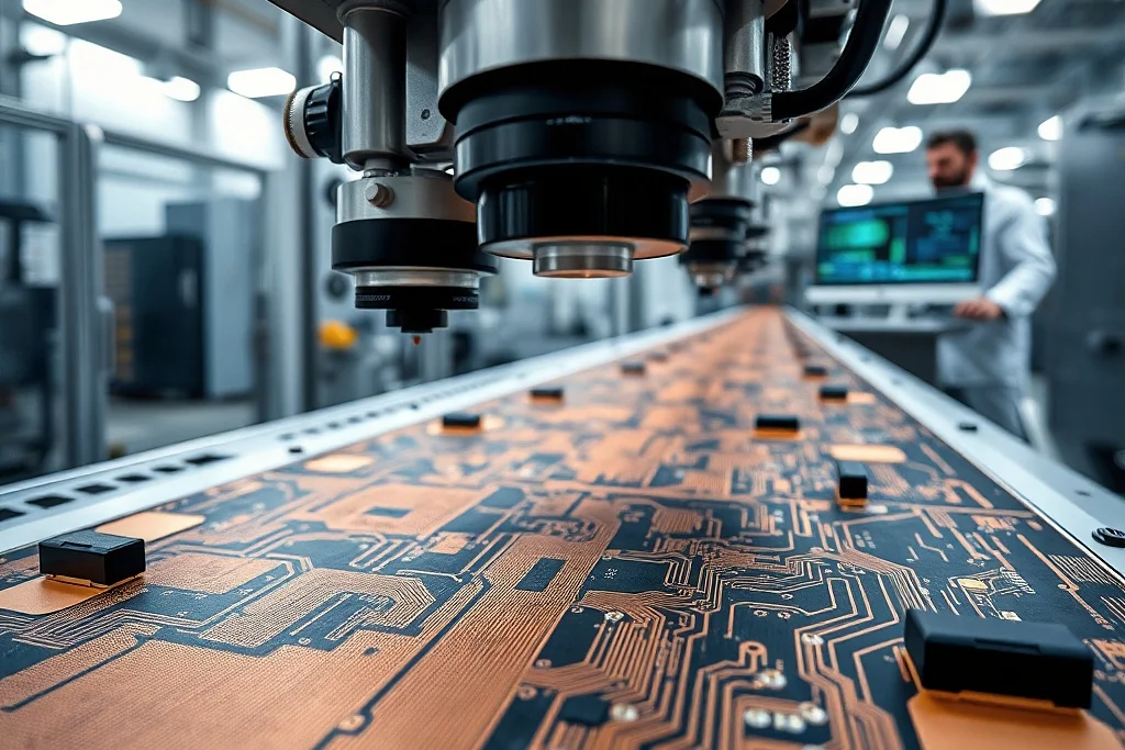
The SPI inspection process begins after solder paste has been printed onto the PCB. The board enters the SPI machine, where high-resolution cameras and measurement systems capture detailed information about the solder paste deposits.
Modern SPI systems typically use 3D inspection technology to analyze the shape and volume of solder paste deposits. The collected data is compared with the expected values defined in the production program.
If the system detects deviations, such as incorrect paste volume, insufficient height, or inaccurate positioning, it generates an inspection report and identifies the problematic area on the PCB.
This allows production teams to immediately adjust the solder paste printing process, clean the stencil, or correct machine parameters before defective boards continue through the assembly line.
Which Defects Can SPI Systems Detect?
Solder Paste Inspection systems are designed to identify a wide range of printing-related defects that can affect PCB assembly quality. Common issues detected by SPI technology include:
- insufficient solder paste volume
- excessive solder paste application
- incorrect solder paste height
- incorrect paste position on PCB pads
- missing solder paste deposits
- uneven solder paste distribution
- solder paste shape irregularities
- problems caused by incorrect stencil printing parameters
Detecting these defects before component placement significantly reduces the risk of producing faulty electronic assemblies and helps maintain stable production quality.
The Role of SPI in SMT Manufacturing
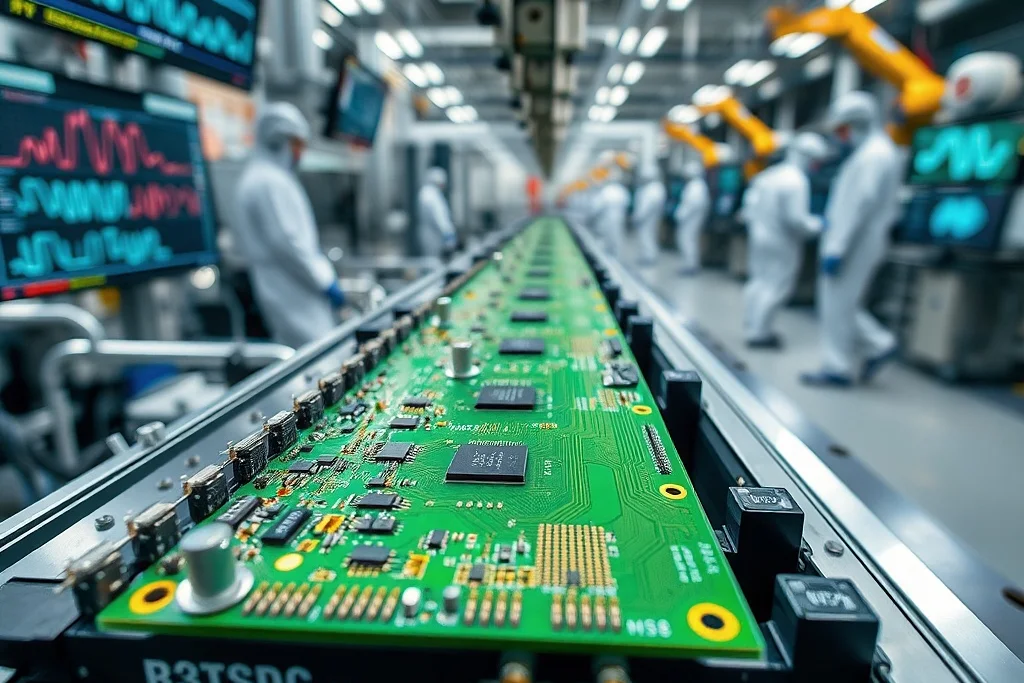
Surface Mount Technology enables manufacturers to produce highly compact electronic assemblies with thousands of components placed on a single PCB. However, the smaller the components become, the less tolerance there is for manufacturing variations.
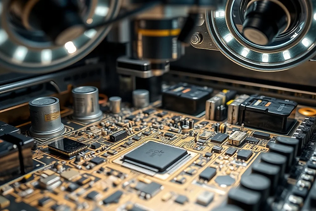
In modern SMT production, components such as microprocessors, sensors, and miniature passive components require extremely precise soldering conditions. Even a small difference in solder paste volume can affect electrical performance and long-term reliability.
SPI provides manufacturers with accurate information about the solder printing process and allows them to maintain stable production parameters. This leads to fewer defects, reduced rework, and improved product quality.
Advantages of Implementing SPI Inspection
Early Detection of Production Problems
One of the biggest advantages of SPI is the ability to identify problems immediately after solder paste printing. Detecting defects at this stage is significantly more efficient than discovering them after component placement or final testing.
Early detection reduces material waste and prevents defective assemblies from moving further through the production process.
Improved Production Stability
SPI systems continuously monitor solder paste printing quality and provide valuable data about process performance. This allows manufacturers to identify trends, prevent recurring issues, and maintain consistent production results.
Reduced Manufacturing Costs
By preventing defects before they become more expensive problems, SPI helps reduce repair costs, production downtime, and unnecessary material consumption.
A stable solder paste printing process also improves overall equipment efficiency and increases manufacturing productivity.
Better Quality Control Data
Modern SPI systems generate detailed inspection reports that can be integrated with manufacturing management systems. These reports provide valuable information for process optimization and quality analysis.
SPI and Industry 4.0 Manufacturing
With the development of Industry 4.0, SPI systems are becoming increasingly connected and intelligent. Modern solutions can communicate with production equipment, collect real-time data, and support automated process adjustments.
Advanced SPI systems combined with data analytics and machine learning can help manufacturers predict potential problems and improve production efficiency.
This makes SPI an important part of smart factories where automation, traceability, and continuous improvement are essential.
SPI Compared to AOI and Other Inspection Methods
Although SPI and Automated Optical Inspection (AOI) are both used for quality control in PCB manufacturing, they inspect different stages of the production process.
SPI focuses specifically on the solder paste printing process before component placement. It measures the quality of solder paste deposits and ensures correct preparation for assembly.
AOI is performed later in the manufacturing process and focuses on detecting visible defects in assembled PCBs, such as incorrect component placement or soldering problems.
Together, SPI and AOI provide a comprehensive inspection strategy that improves quality throughout the entire SMT production process.
Choosing the Right SPI Solution
Selecting the right SPI system depends on several factors, including PCB complexity, production volume, required inspection accuracy, and integration possibilities with existing manufacturing equipment.
A reliable SPI solution should provide accurate measurements, fast inspection cycles, user-friendly operation, and detailed reporting capabilities.
For manufacturers producing advanced electronic assemblies, investing in high-quality SPI technology is an important step toward improving reliability, reducing defects, and achieving efficient production processes.
Conclusion
Solder Paste Inspection is a crucial technology for maintaining quality in modern PCB assembly. By accurately measuring solder paste application and identifying problems before component placement, SPI systems help manufacturers prevent defects and improve production efficiency.
As electronic devices continue to become smaller and more complex, precise control of the SMT manufacturing process becomes increasingly important. Together with other inspection and testing technologies, SPI provides manufacturers with the ability to produce reliable, high-quality electronic products while reducing costs and improving overall production performance.